An Introduction to Quantum Dot Photodetectors
In the ever-evolving field of nanotechnology, few innovations hold as much promise as quantum dots (QDs). These semiconductor nanocrystals are at the forefront of a technological leap, particularly in the realm of optoelectronics. For Indian researchers and professionals in the high-tech industry, understanding the synergy between **quantum dots** and **photodetectors** is crucial. It represents a significant opportunity to drive innovation in everything from consumer electronics to advanced scientific instrumentation.
A photodetector is a sensor that converts light (photons) into an electrical signal. Traditional photodetectors, often made from silicon, have served us well but come with limitations in sensitivity, spectral range, and manufacturing cost. This is where **quantum dots for photodetector device fabrication** come into play. By integrating QDs as the active light-absorbing material, we can create next-generation light sensors that are not only more powerful but also cheaper and more versatile to produce.
This article delves into the core principles, benefits, and applications of QD-based photodetectors, with a special focus on their relevance to the burgeoning R&D and industrial landscape in India. We will explore how this **nanotechnology** is paving the way for superior **light detection**, advanced **imaging sensors**, and a new class of **photonic devices**.
Why Researchers are Turning to Quantum Dots
The unique properties of quantum dots offer tangible advantages for photodetector **device fabrication** and performance. Here’s a breakdown of the key benefits for researchers:
-
Unprecedented Tunability
The most remarkable feature of quantum dots is their size-tunable bandgap. By simply altering the size of the nanocrystal, researchers can precisely control the wavelength of light it absorbs. This allows for the design of photodetectors tailored for specific applications, from deep UV to far-infrared, a feat difficult to achieve with conventional **semiconductor** materials.
-
High Quantum Efficiency
Quantum dots can exhibit very high internal quantum efficiencies, meaning they are exceptionally good at converting absorbed photons into electron-hole pairs. This translates to highly sensitive **light sensors** capable of detecting even faint light signals, crucial for applications in medical imaging and scientific research.
-
Cost-Effective, Solution-Based Fabrication
Unlike traditional semiconductors that require expensive, high-vacuum deposition techniques, quantum dots can be processed in a liquid solution. This opens the door to low-cost, scalable manufacturing methods like spin-coating and inkjet printing. For a country like India, aiming to build a competitive electronics manufacturing ecosystem, this is a game-changing advantage in **optoelectronics**.
-
Broad Spectral Absorption
Beyond their tunable peak absorption, QDs also have a broad absorption spectrum. This means a single type of QD photodetector can operate over a wide range of wavelengths, making them versatile for applications like spectrometry and multi-spectral imaging.
Industry Applications and Future Scope
High-Resolution Imaging Sensors
The small size and high efficiency of QDs allow for the creation of image sensors with higher pixel densities and greater sensitivity than current CMOS/CCD technologies. This is critical for medical imaging (e.g., X-ray detectors), scientific cameras, and high-performance surveillance systems.
Consumer Electronics
QD photodetectors can be integrated into smartphones and wearable devices as highly accurate ambient light sensors, proximity sensors, and even health monitors (e.g., pulse oximeters). Their low-cost fabrication makes them ideal for the mass market.
Optical Communication
In data centers and telecommunications, high-speed photodetectors are essential. QD-based detectors can be engineered to operate at key communication wavelengths (e.g., 1550 nm), offering a low-cost, high-performance alternative for next-generation **photonic devices**.
Environmental Monitoring
Custom-tuned QD photodetectors can be used to build compact, portable spectrometers for detecting pollutants in the air or water. Their ability to target specific absorption lines makes them highly effective for environmental sensing and agricultural tech.
Solar Energy
While not strictly a photodetector, the principles of light absorption are the same. Quantum dots' broad absorption spectrum can be harnessed to improve the efficiency of photovoltaic cells, capturing more energy from sunlight. This is a key area of **nanotechnology** research for sustainable energy.
Machine Vision & Robotics
Advanced robotics and autonomous systems rely on sophisticated **imaging sensors**. QD photodetectors can provide the high-speed, high-dynamic-range imaging needed for these systems to perceive and navigate their environment effectively.
The Indian Opportunity in Quantum Dot Optoelectronics
India's journey towards becoming a global hub for electronics and semiconductor manufacturing is gaining momentum. Initiatives like the National Quantum Mission and 'Make in India' are creating a fertile ground for deep-tech innovation. For researchers in **nanotechnology** and **optoelectronics**, this is a golden era. The development of **quantum dots for photodetector device fabrication** aligns perfectly with national priorities.
The demand for advanced **light sensors** is exploding across various sectors in India – from healthcare to defense and telecommunications. By focusing on solution-processable **device fabrication** techniques, Indian labs and companies can bypass the capital-intensive infrastructure required for traditional silicon fabs. This democratization of manufacturing could lead to a thriving domestic industry for specialized **photonic devices**, reducing reliance on imports and creating high-value jobs. The focus should be on creating intellectual property around novel QD materials and their integration into practical, high-performance **photodetectors**.
Frequently Asked Questions
Quantum dots are semiconductor nanocrystals, typically between 2-10 nanometers in size. Their tiny size gives them unique quantum mechanical properties, most notably the ability to emit light of specific frequencies if electricity or light is applied to them. This frequency can be precisely tuned by changing the dot's size, shape, and material.
Quantum dots are excellent for photodetectors due to their tunable bandgap, high quantum efficiency, broad spectral absorption, and solution-processability. This allows for the creation of highly sensitive, low-cost photodetectors that can be tailored for specific light wavelengths, from ultraviolet to infrared.
Device fabrication refers to the process of constructing the photodetector. For QD photodetectors, this often involves layer-by-layer deposition of materials, including the quantum dot active layer, onto a substrate. Common techniques include spin-coating, inkjet printing, and other solution-based methods which are often simpler and more cost-effective than traditional semiconductor fabrication.
Absolutely. With the Indian government's focus on 'Make in India' and boosting domestic electronics manufacturing, there is a significant push for R&D in advanced materials like quantum dots. Researchers and startups in India have a great opportunity to innovate in areas like low-cost solar cells, advanced medical imaging sensors, and next-generation displays and lighting.
Related Products for Your Research

Perovskite Quantum Dots, Cadmium Free, Hydrophobic (450±15 nm to 690±15 nm)
View Product
CdSe/ZnS(core/shell) Quantum Dots, Powder, Hydrophobic (530 ± 5 nm to 650 ± 5 nm)
View Product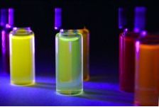
CdTe Quantum Dots, powder, hydrophilic (510 ± 5 nm to 600 ± 5 nm)
View Product
ZnCdSeS Quantum Dots, low-Cd, hydrophobic (540 ± 5nm to 610 ± 5nm)
View ProductReady to Innovate?
Advance your research in optoelectronics and nanotechnology with high-quality quantum dots. Contact our specialists to discuss your specific device fabrication needs.
Contact Us