Printing the Future: The Nanosilver Revolution in India
In an era where the 'Make in India' initiative is propelling the nation towards becoming a global manufacturing powerhouse, a quiet revolution is taking place at the microscopic level. This revolution is driven by advanced materials, and at its forefront is **nanosilver ink**. For researchers, engineers, and innovators across India, this technology represents a monumental leap forward, particularly in the field of **printed electronics**.
Traditional electronics manufacturing is a rigid, complex, and often wasteful process. It involves etching circuits onto silicon wafers or fiberglass boards, a subtractive method ill-suited for the flexible, lightweight, and disposable devices the modern world demands. Printed electronics flips this paradigm on its head. It's an additive process, much like an office inkjet printer laying down text, but instead of ink, it uses functional materials—like **nanosilver conductive ink**—to print circuits onto virtually any surface, from plastic films and paper to textiles and glass.
This guide is designed for the Indian scientific and industrial community. We will explore the science behind **silver nanoparticle ink**, its profound benefits, its diverse applications, and the immense opportunities it unlocks for creating the next generation of **flexible electronics** right here in India. Whether you are in a university lab or an industrial R&D department, understanding **nano printing** is no longer optional; it's essential for staying at the cutting edge.
Key Benefits for Researchers & Industry
Exceptional Conductivity
Nanosilver inks provide electrical conductivity that rivals bulk silver, ensuring high-performance electronic traces essential for reliable **nano circuits** and efficient devices.
Low-Temperature Curing
Unlike traditional materials, nanosilver sinters at low temperatures (often below 150°C). This is a critical advantage for **flexible electronics**, as it allows printing on heat-sensitive substrates like PET, paper, and textiles.
Process Versatility
**Silver inkjet** and aerosol jet printing allow for high-resolution, direct-write fabrication, enabling rapid prototyping and complex circuit designs without the need for expensive masks or tooling.
Mechanical Flexibility
The resulting conductive traces are inherently flexible and can withstand bending and stretching, making them ideal for wearable sensors, flexible displays, and other conformable electronics.
Transforming Industries: Applications of Nanosilver Ink
Wearable Health Sensors
Printing circuits directly onto textiles or flexible patches to create lightweight, comfortable sensors for monitoring ECG, temperature, and other vitals. This is a key area for **nanosilver ink for printed electronics applications**.
Smart Packaging & RFID
Integrating low-cost RFID antennas and sensors into packaging for supply chain tracking, anti-counterfeiting, and consumer engagement. **Conductive printing** makes this scalable.
Flexible Displays & Lighting
Creating the transparent conductive electrodes needed for OLED displays and lighting panels on flexible substrates, paving the way for rollable screens and conformable light sources.
Photovoltaics (Solar Cells)
Printing the fine-line metallic grids (fingers and busbars) on silicon and next-gen perovskite solar cells with higher precision and lower material waste than screen printing.
In-Mold Electronics (IME)
Printing circuits onto a flat sheet that is then thermoformed and injection-molded, seamlessly integrating electronics into 3D plastic parts for automotive and appliance interfaces.
Rapid Prototyping
For R&D labs in India, **electronic ink** allows for the creation of functional **nano circuit** prototypes in hours instead of weeks, dramatically accelerating innovation cycles.
The Indian Advantage: Seizing the Printed Electronics Opportunity
The convergence of India's demographic dividend, its burgeoning tech ecosystem, and strong government support creates a fertile ground for **printed electronics**. The National Policy on Electronics (NPE) 2019 aims to position India as a global hub for Electronics System Design and Manufacturing (ESDM). Technologies like **nanosilver ink** are critical to achieving this vision.
Key opportunities for Indian researchers and industries lie in customization and application development. While global players may lead in bulk material manufacturing, India's strength is in its engineering talent and its vast, diverse market. Developing bespoke **conductive ink** formulations for specific local needs—such as low-cost medical sensors for rural healthcare or robust electronics for the agricultural sector—is a significant area of potential. Research institutions like the IITs, IISc Bangalore, and national labs are already making strides in material science. Collaborations between these institutions and industry are crucial for translating lab-scale innovations into commercially viable products.
Furthermore, the demand for smart devices, IoT, and wearables is exploding in India. By developing domestic capabilities in **nano printing** and **flexible electronics**, India can reduce its reliance on imported components, build a self-reliant supply chain, and capture a significant share of this high-growth market. The journey starts with mastering the foundational materials, such as high-purity **silver nanoparticle ink** precursors, which are essential for high-performance applications.
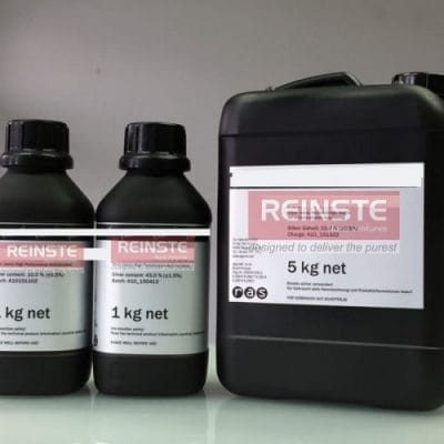
Essential Materials for Your R&D
To begin your journey in printed electronics, high-quality precursor materials are essential. These nanoparticles and solutions form the basis for formulating high-performance conductive inks.


Frequently Asked Questions
Ready to Innovate?
Take the next step in your research or product development. Explore our range of high-purity nanomaterials or contact our experts to discuss your specific application needs.
Get in Touch