The Dawn of Additive Electronics Manufacturing
The world of electronics is shrinking. As devices become smaller, faster, and more integrated into our lives, the demand for more sophisticated, cost-effective, and flexible manufacturing methods has skyrocketed. Traditional techniques, like photolithography, have been the bedrock of the semiconductor industry for decades. However, these subtractive methods are often complex, expensive, and generate significant chemical waste. Enter a revolutionary alternative: microcircuit copper ink, a cornerstone of additive manufacturing and an ultra-fine print solution that is set to redefine electronic circuit fabrication.
For Indian researchers, startups, and established R&D labs, this technology represents a monumental leap. It democratizes the production of high-performance electronics, enabling rapid prototyping and manufacturing without the need for billion-dollar fabrication plants. At its core, this technology leverages nano ink micro print capabilities, using specialized inks containing copper nanoparticles to print intricate conductive pathways onto various substrates, from rigid boards to flexible plastics. The result is a high-precision nanoscale conductor film, forming the very arteries of modern electronic devices.
Why Researchers in India Should Be Excited
The adoption of advanced copper patterning techniques using nano-inks offers tangible benefits that align perfectly with India's "Make in India" and "Digital India" initiatives. Here’s what makes this microelectronics ink a game-changer:
- Cost-Effectiveness: Additive manufacturing drastically cuts down on material waste. You only print what you need, making it significantly cheaper than etching away excess copper from a board.
- Unmatched Precision: The technology achieves incredible copper inkjet resolution, allowing for the creation of ultra-fine lines and dense circuitry essential for compact and powerful devices.
- Speed and Agility: Researchers can go from digital design to a functional prototype in hours, not weeks. This accelerates innovation cycles and allows for rapid iteration and testing.
- Substrate Versatility: Unlike rigid PCBs, precision electronics coat technology can be applied to flexible, stretchable, and even 3D-printed surfaces, paving the way for wearable tech, flexible displays, and IoT sensors.
- Environmental Friendliness: By eliminating harsh chemical etchants and reducing material consumption, this process is far more sustainable than traditional methods.
From the Lab to the Real World: Key Applications
The potential uses for this high-resolution ink are vast and transformative. Here are some of the most promising areas where this technology is making an impact:

Flexible Electronics & Wearables
Printing conductive circuits on flexible polymers enables the creation of smart clothing, wearable health monitors, and rollable displays. The printed device layer is durable enough to withstand bending and stretching.

RFID Antennas & IoT Devices
The ability to rapidly print RFID antennas directly onto packaging or products at low cost is a huge boon for logistics and retail. It's a key enabler for the massive deployment of IoT networks.

High-Density Sensors
The ultra-fine print solution allows for the design of complex, multi-layered sensors for medical, environmental, and industrial applications with enhanced sensitivity and a smaller footprint.
The Indian Opportunity: A New Wave of Electronics Manufacturing
India stands at a critical juncture. With a booming digital economy and a strategic push towards self-reliance in electronics manufacturing, technologies like nano copper ink for ultra-fine circuit microprinting are not just an academic curiosity—they are a national asset. The ability to create a nanoscale conductor film with high precision opens doors for domestic innovation in sectors like defense, aerospace, telecommunications, and consumer electronics.
The key is the remarkable copper inkjet resolution that can now be achieved. This allows Indian companies to compete on a global scale, producing high-density interconnects (HDIs) and complex multi-layer circuits without relying on foreign fabs. As the ecosystem for microelectronics ink matures, we will see a surge in custom-designed chips, specialized sensors, and innovative electronic products tailored for the Indian market. This is the essence of the nano ink micro print revolution: empowering local talent with global capabilities.
Featured Materials for Your Research
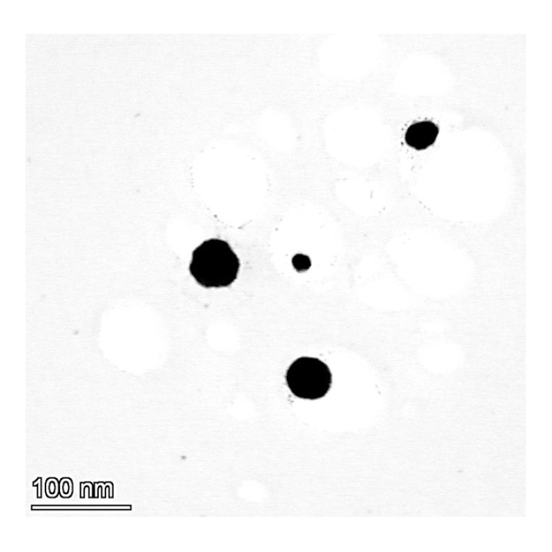
Copper nanoparticles aqueous dispersion 70nm (3wt% and 10wt%)
View Product →
99.9% Silver Coated Copper Superfine Powder For Conductive Ink
View Product →
High Purity Copper Nanopowder
View Product →
Copper Nanowires
View Product →Frequently Asked Questions
Have a Question or a Project in Mind?
Our team of experts is ready to help you leverage the power of nano materials. Contact us for collaborations, product inquiries, or technical support.