An Introduction to the Conductive Revolution
Imagine a world where electronic circuits are no longer confined to rigid green boards but are printed onto flexible plastics, textiles, and even paper. This is not science fiction; it is the reality being built today with conductive ink. For researchers and industries across India, from the bustling tech hubs of Bengaluru to the academic corridors of the IITs, the advent of printable electronics represents a monumental leap. At the heart of this revolution lies a critical component: the nano pigment, a microscopic marvel that dictates the performance and potential of these futuristic inks.
Conductive inks are essentially functional inks that carry electrical currents. They are formulated by suspending conductive particles, such as silver, copper, or—increasingly—advanced carbon forms like nano carbon black, within a binder system. When this ink is applied to a substrate via methods like inkjet printing or screen printing, and subsequently cured, it forms a solid, conductive trace. The efficiency of this trace, its print conductivity, is paramount and is directly influenced by the quality of the nano dispersion—the art and science of keeping these tiny particles perfectly separated and suspended.
This article serves as a comprehensive guide for the Indian R&D community. We will delve into the nuances of ink formulation, explore the benefits of using high-performance carbon additives, and showcase the diverse printing applications that are set to redefine electronics manufacturing in India and beyond.
Why Researchers Should Focus on Conductive Inks
For the Indian scientific community, mastering conductive ink technology offers a gateway to innovation, patents, and commercially viable products. Here are the key benefits:
-
Cost-Effective Material Science
Utilizing nano carbon black for conductive inks provides a significantly cheaper alternative to traditional silver-based inks. This cost advantage allows for more extensive experimentation and opens up possibilities for mass-market applications, a key consideration for India's price-sensitive market.
-
Pioneering Flexible Electronics
The development of flexible, stretchable, and wearable electronics is a global megatrend. Expertise in conductive ink formulation allows researchers to create next-generation devices like smart textiles, wearable health monitors, and flexible displays, positioning India as a leader in this high-growth sector.
-
Advancing Additive Manufacturing (3D Printing)
Conductive inks are not just for 2D surfaces. They are integral to the 3D printing of functional electronic components. Researchers can innovate in creating multi-material 3D printers that can embed electronic ink directly into structural parts, revolutionizing prototyping and custom device manufacturing.
-
Sustainable and Green Electronics
Printing electronics is an additive process, meaning it adds material only where needed. This drastically reduces waste compared to traditional subtractive methods (like etching PCBs). Formulating with benign materials like carbon further enhances the green credentials, aligning with global sustainability goals.
Key Printing Applications and Industries
RFID and Smart Packaging
The logistics and retail sectors in India are booming. Screen printing of conductive ink antennas for RFID tags offers a low-cost solution for inventory management, anti-counterfeiting, and interactive packaging. A stable nano dispersion is key to producing millions of tags with consistent performance.
Wearable Technology & E-Textiles
From fitness trackers integrated into clothing to biomedical sensors that monitor vital signs, wearable tech is a major opportunity. Formulating a flexible conductive ink that can withstand stretching and washing is the primary challenge, making the choice of polymer binder and carbon additive critical.
Printed Circuit Boards (PCBs) & Prototyping
For rapid prototyping, inkjet printing with conductive ink allows engineers to create and test circuit designs in hours, not weeks. This accelerates the innovation cycle for startups and research labs. High print conductivity is essential for these functional prototypes to work reliably.
Sensors and IoT Devices
The Internet of Things (IoT) requires billions of low-cost sensors. Conductive inks can be used to print sensors for detecting pressure, temperature, humidity, and various gases. The versatility of the printing application allows these sensors to be placed on virtually any surface.
Solar Cells (PV)
In the photovoltaic industry, conductive inks are used to print the current-collecting grids on solar cells. Using advanced nano pigment formulations can improve efficiency and reduce manufacturing costs, directly supporting India's ambitious renewable energy targets.
Flexible Displays and Lighting
OLED and e-paper displays require transparent conductive films. While ITO is the incumbent, carbon-based conductive inks (like those using graphene or CNTs) are being heavily researched as flexible, more robust alternatives. This is a high-potential area for advanced materials research.
Opportunities and Trends for Conductive Inks in India
The Indian government's "Make in India" and "Digital India" initiatives create a fertile ground for technologies like printable electronics. The demand for low-cost, domestically produced electronic components is skyrocketing. Researchers and businesses that focus on the ink formulation of conductive ink are poised to capitalize on several key trends.
One major trend is the shift towards sustainable and cost-effective materials. While silver has long been the gold standard for high conductivity, its price volatility is a major deterrent. This is where nano carbon black for conductive inks in printing comes into play. As a carbon additive, it offers a balance of good print conductivity, excellent chemical stability, and a significantly lower cost. Indian labs that can perfect the nano dispersion of these carbon pigments will have a distinct competitive advantage, enabling the production of affordable electronic ink for mass-market products.
Another significant opportunity lies in customizing ink solutions for specific printing applications. The requirements for a high-resolution inkjet printing ink are vastly different from a high-throughput screen printing paste. This necessitates deep expertise in adjusting viscosity, solvent systems, and particle loading. The Indian market, with its diverse industrial base from automotive to healthcare, requires bespoke solutions, creating a market for specialized ink formulators who can bridge the gap between raw nano pigment supply and end-user application.
Recommended Materials for Your Research

Conductive Carbon Black
View Product →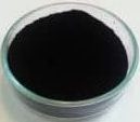
Carbon Black nanopowder (50g)
View Product →
Carbon Mesoporous Materials
View Product →
Carbon Black Powder
View Product →Ready to Innovate?
Advance your research with high-purity nano materials. Explore our extensive catalog or contact our experts for custom solutions.
Explore Hiyka.comFrequently Asked Questions
A conductive ink is a specialized ink that results in a printed object which conducts electricity. It is formulated by dispersing conductive materials like nano carbon black, silver flakes, or copper nanoparticles into a polymer resin or solvent. Once printed and cured, it forms conductive pathways, essentially creating printed electronic circuits.
Nano dispersion is critical because it ensures that the conductive nano pigments are uniformly distributed throughout the ink without agglomerating. A stable nano dispersion leads to consistent and reliable print conductivity, smoother printing processes (preventing nozzle clogging in inkjet printing), and stronger adhesion to the substrate. Poor dispersion results in erratic electrical performance and printing defects.
In many low-power and flexible electronics applications, yes. Conductive inks are ideal for creating flexible circuits, RFID antennas, sensors, and wearable electronics where traditional rigid wires are impractical. However, for high-power applications, traditional copper wiring remains superior due to its lower resistance and higher current-carrying capacity. The choice depends entirely on the specific application's requirements.
Key challenges for researchers in India include sourcing high-purity, consistently sized nano pigments at a viable cost, achieving stable nano dispersion without expensive equipment, and formulating inks that are compatible with a wide range of local substrates and printing technologies. Additionally, optimizing the curing process (temperature and time) to achieve maximum print conductivity without damaging flexible or heat-sensitive substrates is a significant area of research.